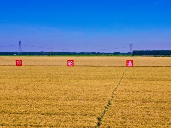
Figure 1. a) SEM image of the chemically derived graphene sheets lying on a SiO2/Si substrate. b) SEM image showing a domain of the hcp PS nanosphere monolayer that masked the graphene sheets. c) SEM image of the large area, interconnected 2D GNRs network etched through an hcp monolayer NSL mask. d) Tapping mode AFM image of a selected typical nanoribbon with width of ca. 12 nm (measured via line scan profile). e) SEM images showing the temporal evolution of the individual dumbbell-like GNRs etched through the isolated pairs of packed nanospheres (top panel) with etching durations of 12 s, 18 s and 24 s. Scale bars in (e): 500 nm. f) Schematic illustration (not to scale) showing the NSL-defined lithographic etching process of graphene sheets.
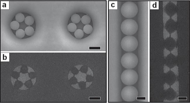
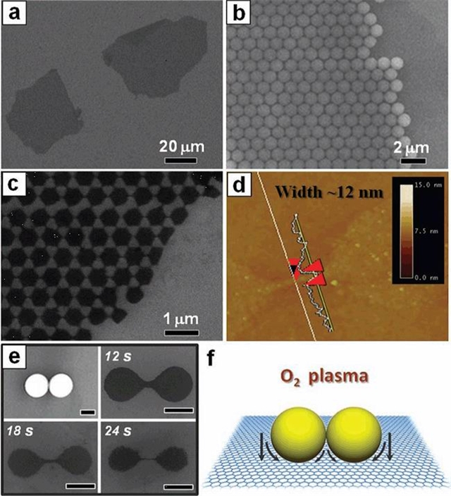
Figure 2. a, c) SEM images showing the well-defined nanosphere pentagons and linear chains formed from ≈ 1 μ m PS nanospheres in the ≈ 3 μ m cylindrical holes of the photoresist and 2 μm spheres in photoresist trenches with ≈ 2 μm width. b, d) SEM images of the pentagonal ring and linear chain architectures of connected GNRs, etched through the corresponding nanosphere masks. Scale bars: 1 μm.
Figure 3. a) Schematic illustration of the on-chip bandgap tuning of graphene through NSL nanopatterning and subsequent O2-plasma etching. b) AFM image of a typical FET device based on the mechanically cleaved single-layer graphene sheet. c) Evolution of the device current–voltage ( Ids – Vds ) characteristics for different etching times (12 s, 18 s, 24 s, and 30 s). d) Evolution of the gate-voltage (Vg)-dependent electrical conductance of the same device upon etching. e) Ids – Vds curves recorded under various Vg for the device after 30 s etching. f) Micro-Raman spectra of the pristine graphene sheet and the resultant GNRs network produced by 30 s of etching.
石墨烯(Graphene)自2004年发现以来,成为凝聚态物理与材料科学等领域的一个研究热点。石墨烯的超高室温载流子迁移率与可剪裁加工的特性,使其成为未来纳米电子学器件的重要候选材料。石墨烯本身是零带隙材料,如果直接用其构筑场效应晶体管(FET)器件,门控效果极其有限,难以实现开关特性。目前的一种解决方案是,把石墨烯裁剪成在横向方向为有限尺寸的石墨烯纳米带结构,电子在横向上受限,纳米带则成为典型的准一维系统,石墨烯的能隙被打开。因此,如何高效、可控地制备石墨烯纳米带(宽度到10 nm左右或以下)是当前该领域的一个充满挑战的重要研究课题。
中科院物理所/北京凝聚态物理国家实验室(筹)表面室SF1组几年来在石墨烯的制备及其能带调控方面开展研究,在过去工作的基础上,最近该组王文龙副研究员、北京大学王恩哥院士和博士生刘磊等与物理所微加工实验室顾长志研究员合作,在石墨烯纳米带的可控制备研究方面取得了重要进展。他们基于二维胶体晶体刻蚀技术,发展出一种简单、高效、可控制备超细石墨烯纳米带的新方法。二维胶体晶体刻蚀又称纳米球刻蚀(NSL),是利用自组装胶体微球作为图形掩膜的一种并行(parallel)刻蚀加工技术,具有操作简便、高产出、成本低廉等显著优点,为未来大批量制备石墨烯纳米带提供了一条有效途径。在NSL法刻蚀裁剪石墨烯的过程中,研究人员巧妙利用了胶体微球空隙中氧等离子体束流的局域各向异性分布,通过细致研究刻蚀工艺与参数,制得了高各向异性的准一维超细纳米带结构。该方法除了能够制备大面积互连的石墨烯纳米带有序阵列之外,还可以通过控制胶体微球的受限自组装,在基片特定位置上制备出不同几何构型的石墨烯纳米带互连结构,展现出了丰富的可调性与良好的可控性。另外,基于NSL刻蚀法的简便与易操作性,他们还将之直接运用到预先制作好的石墨烯FET器件上,通过逐步刻蚀来实现对石墨烯电学性质的“器件原位”(on-chip)动态调控,展示了该方法在石墨烯电子器件研究中的潜在应用价值。相关工作论文发表在近期的《先进材料》(Adv. Mater. 23,1246 (2011)) 上。
该工作得到了国家自然科学基金委、科技部与中科院的支持。(来源:中国科学院物理研究所)
特别声明:本文转载仅仅是出于传播信息的需要,并不意味着代表本网站观点或证实其内容的真实性;如其他媒体、网站或个人从本网站转载使用,须保留本网站注明的“来源”,并自负版权等法律责任;作者如果不希望被转载或者联系转载稿费等事宜,请与我们接洽。