|
|
|
|
|
郑州大学、西湖大学等三位专家讲述基于扫描探针的纳米科学与纳米技术 |
|
|

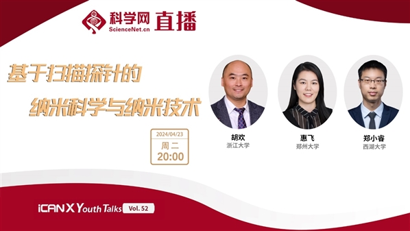
直播时间:2024年4月23日(周二)20:00-22:00
直播平台:

科学网APP
https://weibo.com/l/wblive/p/show/1022:2321325026340003774489
(科学网微博直播间链接)

科学网微博

科学网视频号
北京时间4月23日晚八点,iCANX Youth Talks第五十二期邀请到了浙江大学Huan Hu,郑州大学Fei Hui,西湖大学Xiaorui Zheng三位教授主讲,北京大学Haixia Zhang作为主持人,浙江大学Yang Xu担任嘉宾,期待你一起加入这场知识盛宴。
【嘉宾介绍】

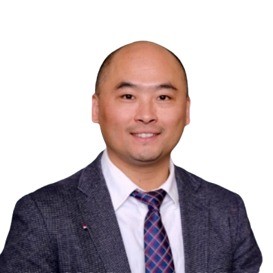
Huan Hu
浙江大学
Special scanning probes and their applications in nanoscale fabrication and measurement
【Abstract】
Atomic force microscope (AFM) is an indispensable technology for nanoscience and nanotechnology featuring nanoscale measurement, manipulation, and fabrication. The key component of AFM is the scanning probe usually made of silicon or silicon nitride that determines in large extent of the functions. In addition to measuring morphology, AFM can measure many other material properties including surface potential, temperature, magnetic properties, modulus, etc. Here, in this talk, I will present three special scanning probes that are developed for different unique applications.
The first is a heated AFM probe that can deposit arbitrarily shaped polymer structures that can later serve as etching mask for patterning solid-state materials such as silicon and 2-D materials. Nanofluidic channels, nano-resonators and nano-transistors can be fabricated by this method without using expensive electron beam lithography or focused ion beam technology with a resolution down to 100 nm.
The second is a nano-spherical probe which is fabricated by implanting helium ions to single-crystal silicon to form a robust and hollow silicon nanosphere. The hollow nanosphere exhibits super low roughness ~ 0.2 nm, almost 100 times smoother than any other 3-D nanofabrication technology (~ 10 nm roughness), which provides advantages in accurate interface measurement in tribology and in improving the quality of 2-D material heterostructures by removing contaminants and bubbles.
The third probe is a high aspect ratio probe that is fabricated by ion induced platinum deposition. This probe has an aspect ration of more than 20:1 and can measure high aspect ratio trenches as well as the surface tension of liquid droplet with sub-micron sizes.
原子力显微镜(AFM)是纳米科学技术不可或缺的技术,能进行纳米尺度的测量、操纵和制造。AFM的关键部件是扫描探针,通常由硅或氮化硅制成,它在很大程度上决定了其功能。除了测量形貌外,AFM还能测量许多其他材料性质,包括表面电位、温度、磁、力学模量等。在这个演讲中,我将介绍三种专为不同独特应用开发的特殊扫描探针。
第一种是可加热AFM探针,能沉积任意形状的聚合物纳米结构,聚合物纳米结构作为刻蚀掩模用于图案化固态材料如硅和二维材料。使用这种方法可以制造纳米流体通道、纳米谐振器和纳米晶体管,而无需使用昂贵的电子束光刻或聚焦离子束技术,分辨率可达100纳米。
第二种是由氦离子注入单晶硅制成的纳米球探针,形成了坚固的空心硅纳米球。空心纳米球的表面粗糙度极低,约为0.2纳米,几乎比任何其他3D纳米制造技术(约10纳米粗糙度)平滑100倍。接近完美的球面提供精确界面测量、空心和光滑表面使得探针非常耐摩,且能通过接触式扫描精准原位去除污染物和气泡改善二维材料异质结。
第三种探针是通过离子诱导的铂沉积制造的高纵横比探针。这种探针的纵横比超过20:1,可以测量高纵横比的沟槽以及亚微米尺寸的液滴表面张力。
【BIOGRAPHY】
Dr. Huan HU is a tenured associate professor at ZJU-UIUC Institute (Joint institute of Zhejiang University and University of Illinois). He received B.S and M.S degrees from Tsinghua University and Ph.D. in University of Illinois at Urbana-Champaign (UIUC) from Electrical and Computer Engineering. He completed his postdoc training in IBM T. J. Watson Research Center in New York. He focuses on advanced nanofabrication and measurement and highly engages in interdisciplinary research. He has published 77 peer-reviewed papers on 45 different journals covering electronics, mechanics, biomedicine, chemistry, and materials. He has 19 granted US patents and 6 granted CN patents. He invented a novel approach of producing robust nano-spherical probes promising for accurate nanoscale interface and mechanical measurement in 2020 and received iCANx summit 2022 excellent paper award. Based on this invention, he founded a startup company that is currently supplying special scanning probes to researchers in tribology, biomedicine, and 2-D materials.
胡欢博士,浙江大学伊利诺伊大学香槟校区联合学院(ZJU-UIUC Institute) 长聘副教授。清华大学学士、硕士,美国伊利诺伊大学厄巴纳香槟校区 (UIUC)电气与计算机工程专业博士。他在纽约IBM T. J. Watson研究中心完成了博士后培训。他专注于先进纳米制造和测量,并积极展开跨学科研究。他在45种不同期刊上发表了77 篇同行评审论文,涵盖电子、机械、生物医学、化学和材料等领域。拥有19项美国专利授权和6项中国专利授权。2020年发明一种生产坚固的纳米球形探针的新方法,能够实现精确的纳米级界面和材料力学测量,获得2022年iCANx峰会优秀论文奖。基于这项发明,他创立了一家科技公司,目前为摩擦学、生物医学、二维材料的研究人员提供特殊的扫描探针。目前担任中国仪器仪表学会微纳器件与系统分会理事、中国微纳技术学会青年委员会委员、中国微纳米测量与仪器分会理事。

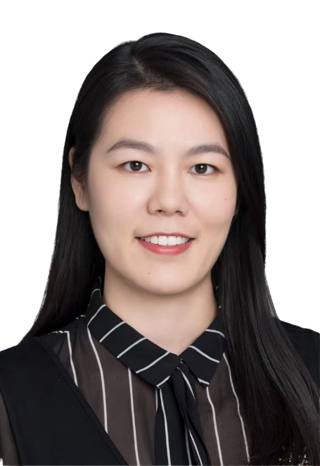
Fei Hui
郑州大学
Application of C-AFM for two-dimensional materials and nanomemristors
【ABSTRACT】
As the size of electronic devices continues to shrink, in-situ characterization methods capable of precisely probing localized properties become increasingly important. Scanning probe microscopy techniques, especially conductive atomic force microscopy (C-AFM), can study local electromechanical properties and play a valuable role in the development of nanoelectronics. This talk first briefly introduces the development of graphene-coated conductive nanoprobes and its reliability characterization related to CAFM technology; Second, it focuses on the application of CAFM technology for the electrical characterization of two-dimensional (2D) materials and memristors, mainly including: i) Study the electrical properties of hexagonal boron nitride (h-BN) prepared by chemical vapor deposition method, e.g., dielectric breakdown characteristics and uniformity of electrical properties; ii) Detect the resistive switching characteristics of h-BN-based memristors and the morphological characterization of conductive filaments in different environments (atmosphere and high vacuum) ; iii) Achieve the emulation of synaptic plasticity behaviors at the nanoscale by combining with device-level electrical testing equipment.
随着电子器件尺寸和介电材料厚度的不断缩减,开发纳米尺度的原位电学等表征技术对研究小尺寸材料和纳米电子器件的电学特性十分重要。扫描探针显微镜(尤其是导电原子力显微镜C-AFM)可以研究局部的机电特性,在纳米电子学的发展过程中发挥重要作用。本报告首先简要介绍石墨烯包覆导电纳米探针的研发及其在C-AFM技术中应用的可靠性表征;其次重点介绍CAFM技术在2D材料和忆阻器中的电学表征应用。具体包含利用CAFM技术:1.研究化学气相沉积法制备的六方氮化硼(h-BN)的电学性质:介质击穿特性和厚度及电学性质均一性;2.在不同环境(大气和真空)下探测h-BN基忆阻器的阻变特性及导电细丝的形态表征;3.通过与器件级别电学测试设备相结合,实现纳米尺度的突触可塑性行为模拟。
【BIOGRAPHY】
Fei Hui is an associate professor of Zhengzhou University in China. Dr. Hui got her PhD degrees in Nanoscience at the University of Barcelona and in Chemistry at Soochow University in 2018. During her PhD, she visited the Massachusetts Institute of Technology (USA) for 12 months and the University of Cambridge (UK) for 6 months. In 2018-2021, she was a postdoctoral fellow at Technion – Israel Institute of Technology. Dr. Hui has published over 60 research papers, 15 of them as first/corresponding author, including Nature Electronics, Advanced Materials, Advanced Functional Materials, Small, among others (Google scholar citation>4200). Dr. Hui have received the Microelectronic Engineering Young Investigator Award (2022), Chinese Government Award for Outstanding Self-financed Students Abroad (2022), Park Systems postdoctoral award (2019), and the Mobility Grant of Royal Society of Chemistry (2016), among others. She serves as an associate editor in Microelectronic Engineering, a member of IEEE EDS Nanotechnology committee (2021-2023), a member of technical committee of the international conferences in the field of electronic materials and devices, such as IEEE-IPFA, IEEE-IPRS and IEEE-IIRW. Her research interests are the development of two-dimensional materials and nanoelectonics.
惠飞,博士,直聘研究员,河南省高层次人才,2022年加入郑州大学材料科学与工程学院。2018年获西班牙巴塞罗那大学和苏州大学双博士学位,2019-2021年在以色列理工学院从事博士后研究。博士期间,先后到美国麻省理工学院(12个月)、英国剑桥大学(6个月)访学。主要研究领域是基于低维材料的神经形态器件和纳米电子技术,发表SCI学术论文60余篇,包括Nature Electronics、Advanced Materials、Advanced Functional Materials等,论文总引用次数>4000次。参与出版专著篇章1部,获授权国家发明专利2件,担任Microelectronic Engineering期刊副主编、以及多个国际学术会议的技术委员会成员(如2024 IEEE EDTM、2023 IEEE IPFA、2023 IEEE IRPS)。获得爱思唯尔微电子工程领域青年研究员奖、2021年度国家优秀自费留学生奖学金、韩国Park Systems AFM奖学金、英国皇家化学会国际交流奖学金(RSC Research Mobility Grant)等。

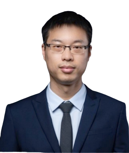
Xiaorui Zheng
西湖大学
Scanning probe technology for low-dimensional opto-electronics
【ABSTRACT】
Progress in nanotechnology depends on the capability to fabricate, characterize and manipulate nanometer-scale structures. However, the existing conventional lithography techniques pose limitations and challenges related to resolution, operational costs, and more importantly, the lack of flexibility to pattern emerging low-dimensional materials such as graphene and transition-metal dichalcogenides.
Since the first patterning experiments performed with a scanning probe microscope in the late 1980s, scanning probe lithography has emerged as an alternative type of lithography for academic research that has provided striking capabilities to pattern three-dimensional relief structures with nanoscale features, the fabrication of the smallest field-effect transistor, or the patterning of proteins with 10-nm feature size.
In this presentation, I will introduce the scanning probe-based fabrication, characterization and manipulation of novel low-dimensional materials and explore their various applications in opto-electronics, including field-effect transistors, diodes, photodetectors, memristors, and low-dimensional ferroelectrics.
纳米技术的进步依赖于制造、表征和操纵纳米级结构的能力。然而,传统的图案化技术在分辨率、灵活性、成本方面存在局限性。更重要的是,当前对石墨烯和过渡金属硫化物等新兴低维材料的操控仍面临挑战。
自20世纪80年代末,扫描探针技术被首次应用于结构的图案化制造,扫描探针光刻已逐渐成为学术研究的前言,它提供了独特的三维图形化制造能力、制造了最小的场效应晶体管、及具有 10 纳米特征尺寸的蛋白质图案等多种应用。
在本次演讲中,我将介绍基于扫描探针的新型低维材料的制造、表征和操纵技术,并探讨其在光电子器件中的各种应用,包括场效应晶体管、二极管、光电探测器、忆阻器和低维铁电等。
【BIOGRAPHY】
Dr. Xiaorui Zheng is currently an Assistant Professor at Westlake University. Dr. Zheng received his Bachelor’s degree at Wuhan University, Master’s degree at Chinese Academy of Sciences and Ph.D at Swinburne University of Technology. After graduate, Dr. Zheng was appointed as a postdoc research fellow at University of California, San Diego, City University of New York and New York University, respectively. Dr. Zheng joined Westlake University in 2020 and started Alien Lab.
Dr. Zheng has been awarded with National Youth Talents Plan and Zhejiang Provincial Talents Plan. Dr. Zheng has been appointed as the reviewer of NSFC and the associate director of Key Laboratory of 3D Micro/Nano Fabrication and Characterization of Zhejiang Province.
郑小睿博士,西湖大学工学院助理教授,独立PI。先后在武汉大学、中国科学院物理研究所、澳大利亚斯威本科技大学获得学位,博士期间获“国家优秀自费留学生奖学金”。2016年起在美国加州大学圣地亚哥分校从事博士后研究,2017年获IBM苏黎世研究中心及瑞士SwissLitho公司研发资助,先后在美国纽约先进科学研究中心、纽约大学从事博士后研究,研究方向为扫描探针制造低维纳米光电器件。2020年9月加入西湖大学工学院,组建先进制造与纳米芯片实验室(Alien Lab),开展独立研究工作。
郑小睿博士曾获国家自然科学基金项目资助,担任国家自然科学基金委员会项目评审专家,及浙江省3D微纳加工和表征研究重点实验室副主任。
【主持人】

Haixia Zhang
北京大学
【研讨嘉宾】

Yang Xu
浙江大学
特别声明:本文转载仅仅是出于传播信息的需要,并不意味着代表本网站观点或证实其内容的真实性;如其他媒体、网站或个人从本网站转载使用,须保留本网站注明的“来源”,并自负版权等法律责任;作者如果不希望被转载或者联系转载稿费等事宜,请与我们接洽。