|
|
|
|
|
洛桑联邦理工学院、宾夕法尼亚大学等三位专家讲述先进等离子技术和器件 |
|
|
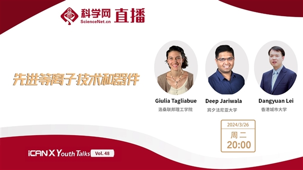
直播时间:2024年3月26日(周二)20:00-22:00
直播平台:

科学网APP
https://weibo.com/l/wblive/p/show/1022:2321325016192925696122
(科学网微博直播间链接)

科学网微博

科学网视频号
北京时间3月26日晚八点,iCANX Youth Talks第四十八期邀请到了洛桑联邦理工学院Giulia Tagliabue,宾夕法尼亚大学Deep Jariwala,香港城市大学Dangyuan Lei三位教授主讲,西安电子科技大学 Rusen Yang作为主持人,北京大学Haixia Zhang教授担任嘉宾,期待你一起加入这场知识盛宴。
【嘉宾介绍】
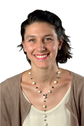
Giulia Tagliabue
洛桑联邦理工学院
Understanding Hot Carrier Processes For Advanced Plasmonic Energy Devices
【Abstract】
In the last decade, plasmonic nanoantennas have revolutionized light manipulation and control at the nanoscale. Interestingly, hot carriers and photoluminescence in metals have opened new pathways for controlling photo(electro)chemical processes and monitoring temperatures. Yet, fundamental questions remain about the microscopic details of these complex light-matter interactions.
We have recently developed a well-controlled experimental platform based on ultrathin monocrystalline gold flakes [1] that, in combination with theory, enables deeper insight into light absorption and emission processes. In particular, I will show results on the hot carrier dynamics in these systems [2] as well as a study unraveling the origin of luminescence in gold, exploring the role of physical confinement, excitation wavelength and temperature [3]. I will then present micro-scale photoelectrochemical measurements clarifying the interplay of hot carrier generation/transport and quantifying the injection probability of high-energy d-band holes at the metal-electrolyte interface [4], connecting it to the ultrafast dynamics of these carriers in monocrystalline metals. Overall, this microscopic insight is critical to advance the design of plasmonic-based energy devices.
在过去的十年里,等离子纳米天线已经彻底改变了纳米尺度上的光操控和控制。有趣的是,金属中的热载流子和光致发光打开了控制光(电)化学过程和监测温度的新途径。然而,关于这些复杂光-物质相互作用的微观细节仍然存在基本问题。
我们最近开发了一个基于超薄单晶金属片的良好控制的实验平台,结合理论,可以更深入地了解光吸收和发射过程。具体而言,我将展示这些系统中热载流子动力学的结果,以及一项研究揭示金属发光起源的研究,探索物理约束、激发波长和温度的作用。然后,我将提出微观尺度的光电化学测量结果,阐明热载流子的产生/输运相互作用,并量化金属-电解质界面处高能d带空穴的注入概率,将其与单晶金属中这些载流子的超快动态联系起来。总的来说,这种微观洞察力对于推进基于等离子体的能源设备的设计至关重要。
【BIOGRAPHY】
Dr. Giulia Tagliabue is a Tenure-track Assistant Professor in the Department of Mechanical Engineering at EPFL. She joined the Engineering faculty in January 2019 where she leads the Laboratory of Nanoscience for Energy Technologies (LNET). She obtained her PhD in Mechanical Engineering from ETH Zurich in 2015. From 2015 to 2018 she was a Swiss National Science Foundation Fellow and she carried on her postdoctoral research jointly at Caltech and the Joint Center for Artificial Photosynthesis (JCAP). Dr. Tagliabue’s research focuses on the study of fundamental mechanisms and nanophotonic-design strategies for light-energy conversion devices, with a special interest for light-energy storage systems. Dr. Tagliabue is the recipient of the First Prize of the Rising Stars of Light Award 2020, the 2021 Early Career Award in Nanophotonics and the 2023 Zellner Prize in Physical Chemistry. In 2020 she was awarded an Eccellenza Grant from SNSF and in 2022 she received an SNSF Starting Grant. She is member of the American Chemical Society (ACS) and the Optical Society of America (Optica). Dr. Tagliabue is currently Managing Editor of the journal Nanophotonics (DeGruyter).
Dr. Giulia Tagliabue是瑞士洛桑联邦理工学院(EPFL)机械工程系的终身助理教授。她于2019年1月加入工程系,并领导着纳米科学能源技术实验室(LNET)。她于2015年从苏黎世联邦理工学院(ETH Zurich)获得机械工程博士学位。从2015年到2018年,她是瑞士国家科学基金会(Swiss National Science Foundation)的研究员,并在加州理工学院(Caltech)和人工光合作用联合中心(JCAP)进行博士后研究。Tagliabue博士的研究重点是研究光能转换设备的基本机制和纳米光子设计策略,特别关注光能储存系统。Tagliabue博士是2020年光之未来新星奖(Rising Stars of Light Award)一等奖、2021年纳米光子学早期职业奖和2023年泽尔纳物理化学奖(Zellner Prize in Physical Chemistry)的获得者。2020年,她获得了瑞士国家科学基金会的Eccellenza资助,2022年获得了瑞士国家科学基金会的启动资助。她是美国化学学会(ACS)和美国光学学会(Optica)的成员。Tagliabue博士目前担任《纳米光子学》(Nanophotonics)杂志的主编。
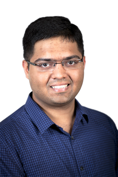
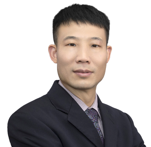
Deep Jariwala
宾夕法尼亚大学
Materials for Low-Power and Extreme-Environment Memory
【ABSTRACT】
Silicon has been the dominant material for electronic computing for decades and very likely will stay dominant for the foreseeable future. However, it is well-known that Moore’s law that propelled Silicon into this dominant position is long dead. Therefore, a fervent search for (i) new semiconductors that could directly replace silicon or (ii) new architectures with novel materials/devices added onto silicon or (iii) new physics/state-variables or a combination of above has been the subject of much of the electronic materials and devices research of the past 2 decades. The above problem is further complicated by the changing paradigm of computing from arithmetic centric to data centric in the age of billions of internet-connected devices and artificial intelligence. Therefore, there is a pressing need for complementing and supplementing Silicon to operate with greater efficiency, speed and handle greater amounts of data. This is further necessary since a completely novel and paradigm changing computing platform (e.g. all optical computing or quantum computing) remains out of reach for now.
The above is however not possible without fundamental innovation in new electronic materials and devices. Therefore, in this talk, I will try to make the case of how novel layered two-dimensional (2D) chalcogenide materials and three-dimensional (3D) nitride materials might present interesting avenues to overcome some of the limitations being faced by Silicon hardware. I will start by presenting our ongoing and recent work on integration of 2D chalcogenide semiconductors with emerging wurtzite structure ferroelectric nitride materials namely aluminium scandium nitride (AlScN). First, I will present on Ferroelectric Field Effect Transistors (FE-FETs) made from 2D materials when integrated with AlScN and make the case for 2D semiconductors in this application. Next, I will introduce our work on Ferroelectric Diode (FeD) devices also based on thin AlScN. In addition, I will also present how FeDs provide a unique advantage in compute-in-memory (CIM) architectures for efficient storage, search as well as hardware implementation of neural networks. Finally, I will present ongoing work and opportunities to extend the application of AlScN memory devices into extreme environments.
硅几十年来一直是电子计算的主导材料,很可能在可预见的未来仍将保持主导地位。然而,众所周知,推动硅走向主导地位的摩尔定律早已不复存在。因此,寻找能直接取代硅的新型半导体,或者将新型材料/器件添加到硅上的新体系结构,或者新的物理/状态变量或以上各项的组合,已成为过去20年电子材料和器件研究的主题。在互联网时代的数十亿连接设备和人工智能的背景下,计算范式从算术中心转变为数据中心,进一步使上述问题变得更加复杂。因此,迫切需要对硅进行补充和增强,以实现更高效、更快速地处理更多的数据。这是因为目前尚无法完全实现全新的、改变范式的计算平台(例如全光计算或量子计算)。
然而,在新型电子材料和器件方面进行基础创新是不可能的。因此,在本次讲座中,我将试图论证新型层状二维(2D)硫化物材料和三维(3D)氮化物材料可能提供有趣途径来克服硅硬件面临的一些限制。我将首先介绍我们关于将2D硫化物半导体与新兴的六方结构铁电氮化物材料,即铝钪氮化物(AlScN)的集成工作。首先,我将介绍基于2D材料与AlScN集成的铁电场效应晶体管(FE-FETs),并阐述在该应用中使用2D半导体的理由。接下来,我将介绍基于薄AlScN的铁电二极管(FeD)器件。此外,我还将介绍FeD在计算内存(CIM)架构中提供的独特优势,用于高效存储、搜索以及神经网络的硬件实现。最后,我将介绍将AlScN存储器件的应用扩展到极端环境的正在进行的工作和机会。
【BIOGRAPHY】
Deep Jariwala is an Associate Professor and the Peter & Susanne Armstrong Distinguished Scholar in the Electrical and Systems Engineering as well as Materials Science and Engineering at the University of Pennsylvania (Penn). Deep completed his undergraduate degree in Metallurgical Engineering from the Indian Institute of Technology in Varanasi and his Ph.D. in Materials Science and Engineering at Northwestern University. Deep was a Resnick Prize Postdoctoral Fellow at Caltech before joining Penn to start his own research group. His research interests broadly lie at the intersection of new materials, surface science and solid-state devices for computing, opto-electronics and energy harvesting applications in addition to the development of correlated and functional imaging techniques. Deep’s research has been widely recognized with several awards from professional societies, funding bodies, industries as well as private foundations the most notable ones being the Optica Adolph Lomb Medal, the Bell Labs Prize, the AVS Peter Mark Memorial Award, IEEE Photonics Society Young Investigator Award, IEEE Nanotechnology Council Young Investigator Award, IUPAP Early Career Scientist Prize in Semiconductors and the Alfred P. Sloan Fellowship. He has published over 150 journal papers with more than 19000 citations and holds several patents.
Deep Jariwala是宾夕法尼亚大学(Penn)电气与系统工程以及材料科学与工程的副教授,也是彼得和苏珊·阿姆斯特朗杰出学者。Deep在印度瓦拉纳西的印度理工学院获得金属工程学士学位,并在西北大学获得材料科学与工程博士学位。在加入宾夕法尼亚大学之前,Deep在加州理工学院担任Resnick奖博士后研究员,开始了自己的研究小组。他的研究兴趣广泛涉及新材料、表面科学和固态器件,主要用于计算、光电子学和能量收集应用,以及相关和功能成像技术的发展。Deep的研究得到了专业学会、资助机构、工业界以及私人基金会的广泛认可,其中最显着的奖项包括Optica Adolph Lomb奖、贝尔实验室奖、AVS Peter Mark纪念奖、IEEE光子学会青年研究员奖、IEEE纳米技术理事会青年研究员奖、国际纯粹与应用物理学会(IUPAP)半导体早期科学家奖和阿尔弗雷德P.斯隆奖学金。他发表了150多篇期刊论文,被引用超过19000次,并持有多项专利。
Dangyuan Lei
香港城市大学
Plasmonic Nanocavities for Enhanced Light-Matter Interaction
【ABSTRACT】
Photonic cavities are man-made resonant structures that can confine light in space, typically in the form of standing waves with certain resonance frequencies. Probably the earliest developed cavity system is a pair of mirrors, termed Fabry–Pérot cavity, which is an indispensable component of lasers and interferometers. While such cavities at the macro-scale are important for many optical devices, they really become shining at the micro- and nanoscale, as exemplified by photonic microcavities made of low-loss dielectric materials and plasmonic nanocavities comprised of resonant metallic nanostructures.
In this talk, I will show our recent discoveries of light-induced electromagnetic asymmetry and optical magnetism in symmetry-broken plasmonic nanocavities and their roles in enhancing surface second-harmonic generation. I will then demonstrate that marrying these small-scale photonic cavities with either photo-switchable molecules or low-dimensional quantum materials can realize high-performance functional devices. Finally, I will share my perspectives on unleashing the full potential of hybrid cavity-quantum-materials paradigms for single-molecule quantum sensing and quantum light emission.
光子腔是人造的共振结构,可以将光束在空间中限制,通常以某些共振频率的驻波形式存在。可能最早开发的腔体系统是一对镜子,称为法布里-珀罗腔,它是激光器和干涉仪不可或缺的组件。尽管宏观尺度上的这种腔体对于许多光学设备至关重要,但它们在微观和纳米尺度上才真正发挥作用,例如由低损耗介质材料制成的光子微腔和由共振金属纳米结构组成的等离子体纳米腔。
在本次演讲中,我将展示我们最近在对称破缺等离子体纳米腔中发现的光诱导电磁不对称性和光学磁性,以及它们在增强表面二次谐波发生中的作用。然后,我将证明将这些小尺度的光子腔与光开关分子或低维量子材料结合起来,可以实现高性能的功能性器件。最后,我将分享我对释放混合腔体-量子材料范式的全部潜力,用于单分子量子传感和量子光发射的观点。
【BIOGRAPHY】
Dangyuan LEI is a Professor in the Department of Materials Science and Engineering at City University of Hong Kong and the Provost’s Visiting Professor of Physics at Imperial College London. He received his PhD degree in Physics from Imperial College London in 2011, with his thesis awarded the Anne Thorne PhD Thesis Prize. His research interest centers on plasmonic nanophotonics, low-dimensional quantum optical materials and the nanoscale cavity-matter interaction and device applications. He has published 220 publications, received 13000 citations and an h-index of 63. Three of his publications have been highlighted as “Editor’s Choice” of Science and “Research Highlights” of Nature Materials respectively. He is an elected member of the Hong Kong Young Academy of Sciences, an OSA Senior Member, a member of SPIE, IOP and PSHK, and a National Science and Technology Expert of MOST. He was the only representative of Hong Kong for the APEC Science Prize for Innovation, Research & Education (ASPIRE, 2021) and received an Outstanding Research Award for Junior Faculty from City University of Hong Kong (2021), Rising Star Lectureship in Materials Science from Hong Kong Institute of Advanced Study (2021), Shanxi Science and Technology Award (2021), Excellent Young Scientists Fund for Hong Kong & Macau from National Natural Science Foundation of China (2020), and Young Innovators Award in 2D Materials from Nano Research (2020).
Dangyuan Lei是香港城市大学材料科学与工程系的教授,也是伦敦帝国学院物理系的校务长访问教授。他于2011年从伦敦帝国学院获得物理学博士学位,其论文荣获安妮·索恩博士论文奖。他的研究兴趣集中在等离子体纳米光子学、低维量子光学材料以及纳米尺度腔体-物质相互作用和器件应用。他发表了220篇论文,被引用13000次,h指数为63。他的三篇论文分别被《科学》杂志和《自然材料》杂志选为“编辑之选”和“研究亮点”。他是香港青年科学院的选举成员,是OSA的高级会员,也是SPIE、IOP和PSHK的成员。他是2021年亚太经合组织创新、研究与教育科学奖(ASPIRE)的香港唯一代表,并获得了香港城市大学的优秀青年教师研究奖(2021年)、香港高等研究学院材料科学领域的新星讲座奖(2021年)、2021年山西科技奖、以及《纳米研究》杂志2D材料领域的青年创新奖(2020年)。
【主持人】
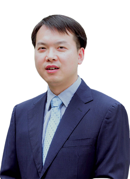
Rusen Yang
西安电子科技大学
【研讨嘉宾】
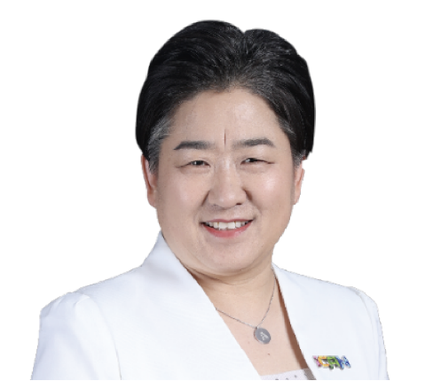
Haixia Zhang
北京大学
特别声明:本文转载仅仅是出于传播信息的需要,并不意味着代表本网站观点或证实其内容的真实性;如其他媒体、网站或个人从本网站转载使用,须保留本网站注明的“来源”,并自负版权等法律责任;作者如果不希望被转载或者联系转载稿费等事宜,请与我们接洽。